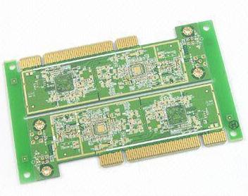
In PCB design, wiring is completed an important step in the design of the products, can be said that in front of the preparatory work is done for it. In the PCB, the wiring to the design process of defining highest, the fine, the largest amount of work.
PCB routing has one side wiring, two sided wiring and multilayer wiring. Wiring way also has two: automatic routing and interactive routing, before the automatic routing can use interactive in advance of the more stringent requirements for wiring, the edge of the input end and the output end should avoid the adjacent parallel, in order to avoid reflection interference. If necessary, the ground wire should be isolated, and the wiring of the two phase adjacent layers should be perpendicular to each other, so that the parasitic coupling can be easily generated.
Automatic routing routing rate, depends on a good layout, wiring rules can be set in advance, including walk the line number of bends and guide through the number of holes and step number of etc.. General first explore type cloth with threads, quickly the short-term connected, then labyrinth wiring, first to cloth line global wiring path optimization, it can according to need to disconnect the cloth line. And try to re wiring, in order to improve the overall effect.
On the high density PCB design has been felt through hole to be less adapted it wasted many valuable routing channels, to solve this contradiction, there has been blind and buried vias technology. It can not only accomplish the conduction hole up many routing channels to make the wiring process become more convenient, more smooth, more perfect, the PCB design process is a complex and simple process, to grasp it very good, still need to the majority of electronic engineering design personnel to go to their own experience, in order to get the true meaning.
1, power, ground handling
Even in the PCB wiring is done very well, but due to the interference of power supply, ground considered not attentive caused will decrease the performance of the product, sometimes even affect the success rate. Therefore, the electrical and ground wiring should be taken seriously, the power of the noise generated by the interference to a minimum, to ensure the quality of products.
For each engaged in the design of electronic products for engineers to understand the cause of the noise between the ground wire and the power line, is only to reduce the noise to make a statement:
(1) it is well known that the power supply and the ground wire add up to the coupling capacity.
(2) try to widen power supply wire width, it is best to ground than power linewidth, their relationship is: ground > power lines, signal lines, usually a signal line width: 0.2 ~ 0.3mm, most fine width can reach 0.05 to 0.07 mm, power line for 1.2 to 2.5 mm
The PCB of the digital circuit can be used to form a loop, that is, a network to be used (such as analog circuits can not be used).
(3) with a large area of copper layer used as ground wire, the printed board is not used on the place to be connected with the ground as a ground wire. Or made of multilayer board, power supply, ground wire each take up a layer.
2, digital circuit and analog circuit of the common processing
Now there are a lot of PCB is no longer a single function circuit (digital or analog circuit), but by the digital circuit and analog circuit mixed. Therefore, we need to consider the mutual interference between them, especially the noise interference on the ground.
High frequency digital circuit, analog circuit of the high sensitivity, the signal line, the high frequency signal line as far as possible away from the sensitive analog circuit device, on the ground, whole PCB on the outside only a node, so must in internal PCB processing, were the problem, and in the plate internal digital and analog ground is actually a separate, they are not connected with each other, but in the PCB and the external connection interface (such as plug, etc.). Digital and analog ground with a little short, please note that there is only one connection point. Also there is no common ground on the PCB, which is determined by the system design.
3, the signal line cloth on the electric (ground) layer
In multilayer printed wiring board, due to the signal line layer without the cloth finish line left already not much, the layers will cause waste will add a certain amount of work to the production, a corresponding increase in the cost of the, in order to solve this contradiction can consider the electric layer wiring. The first consideration should be given to the power layer, followed by the formation. Because it is best to preserve the integrity of the strata.
4, large area of the conductor in the connection of the leg
In the large area of the ground (electric) in, common components of the legs are connected, the connection legs need to be considered, electrical properties, components of the leg pads and the copper surface full connected as well, but on the components of the welding assembly exists some bad risks such as welding connection requires large power heater. It is easy to cause the weld point. So both electrical properties and process, made of cruciferous pad, known for thermal isolation (HSP hield), commonly known as the thermal pad (thermal), so that it can make the welding because the section excessive heat and weld point to the possibility of greatly reduced. The ground layer legs of the multilayer board are treated the same.
5, wiring in the role of network systems
In many CAD systems, wiring is determined by the network system. Dense grid, pathway, although increased, but the step is too small, field maps of large amounts of data, which will inevitably storage space for equipment have higher requirements, and great influence also object computer electronics operation speed. And some of the channels are not valid, such as the components of the leg pads occupied or installed holes, holes are occupied by the fixed and so on. The grid is too sparse, too little pathway has a great influence on the efficiency of the. So there must be a reasonable density grid system to support the wiring.
Standard components between the legs of the distance between 0.1 inches (2.54mm), so the basis of the grid system is generally set to 0.1 inches (2.54 mm) or less than 0.1 inches of the entire multiple, such as: 0.05 inches, 0.025 inches, 0.02 inches, etc..
6, design rule check (DRC)
After the completion of the layout design, need to carefully check the wiring design is consistent with the designers to develop the rule. At the same time, but also to confirm the formulated rules are in line with the printed board production process needs, examination generally have the following aspects:
(1) the line and the line, the line and the element bonding pad, the line and the through hole, the component pad and the through hole, the distance between the through hole and the through hole is reasonable, whether satisfies the production request.
(2) whether the width of the power supply line and the ground wire is appropriate, and whether the power supply and the ground wire are tightly coupled (low wave impedance)? Is there a place where the PCB can be widened.
(3) for the key signal lines to take the best measures, such as the length of the shortest, plus protection line, the input line and the output line is obviously separate.
(4) analog circuit and digital circuit part, whether there is a separate ground wire.
(5) after the addition of graphics in the PCB (such as icon, note) whether the signal will cause short circuit.
(6) modify some of the undesirable alignment.
(7) is there a process line on the PCB? Resistance welding is in line with the requirements of the production process, solder resist size is appropriate, whether the character mark on the device pad, so as not to affect the quality of electrical installation.
(8) power supply in multilayered stratigraphic frame edge is reduced, such as power formation of copper foil exposed outer plate easy to cause a short circuit.
7, check whether there is an acute angle, impedance discontinuities etc.
(1) for high-frequency current, when the conductor corner presents a right angle or acute angle, near the corner of the site, magnetic flux density and electric field intensity is higher, strong electromagnetic wave radiation, and the inductance of the here will be relatively large inductance will also than obtuse or rounded to some big.
(2) bus for digital circuit wiring, wiring is obtuse or rounded corners, wiring occupied area is relatively small. At the same line spacing, the width of the line spacing is 0.3 times smaller than that of the right angle.
8, check 3W, 3H principle
(1) clock, reset, 100M signal and some key bus signal and other signal lines must meet the 3W principle, the same layer and adjacent layer no longer parallel to the line, and the link on the hole as little as possible.
(2) with high speed signal hole number, some devices guide book on General of high-speed signal a hole quantity requirements more stringent, consulting interconnection principle is in addition to the through hole to pin the fanout, is strictly prohibited in the inner play redundant vias, they cloth 8g PCIe 3.0 walk the line, also played four holes, no problem.
(3) clock in the same layer and high speed signal center distance to be strictly satisfied 3H (H is the wiring layer to the return line spacing plane); signal of adjacent layers of non overlapping, advice and also satisfy the 3H principle, on the crosstalk problem, tool can check.